Magnetron sputtering is a thin film deposition technique used extensively in materials science, optics, and electronics to fabricate different thin films with special functions due to its high sputtering rate and low deposition temperature requirement. This article discusses the application of magnetron sputtering in the fabrication of thin films.
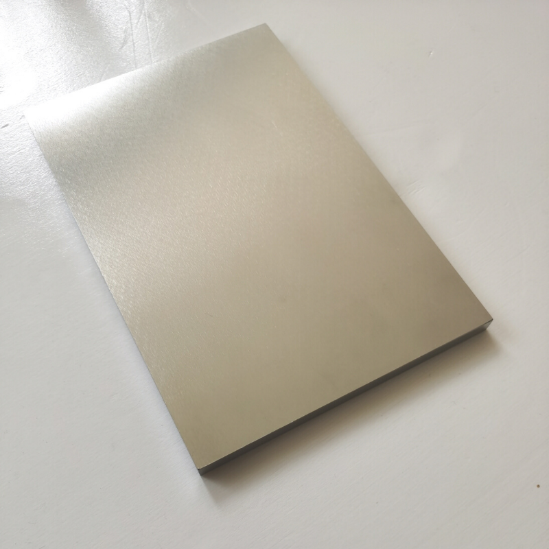
Image Credit: White_Fox/Shutterstock.com Magnetron Suppliers
Thin films play a crucial role in the fabrication of several components and devices, such as protective coatings, integrated circuits, solar cells, and optical/decorative/large-area coatings.
Precise control over the film composition, thickness, and uniformity and the ability to deposit different materials over several substrates are the other key advantages of this thin-film coating technology over other deposition techniques.
Sputtering involves the ejection of molecules/atoms from a solid target material due to the high-energy particle/ion bombardment. During this process, the kinetic energy from the incident ions is transferred to the targeted atoms, which results in a chain reaction of collisions within the target surface.
The targeted atoms are ejected from the target surface through evaporation when sufficient kinetic energy is transferred to overcome the binding energy of the targeted atom. Eventually, the ejected atoms can be deposited on an adjacent substrate.
In magnetron sputtering, positively charged ions, such as argon gas, are accelerated using an electric field towards a negatively charged target/cathode for targeted atom ejection. The ion bombardment process leads to both target atom removal and secondary electron emission from the sputtering target.
These emitted electrons can ionize the sputtering gas, which contributes to the plasma generation that sustains the entire sputtering process.
The sputtering process is primarily dependent on the mass of the ions, the angle of incidence, target atoms, and incident ion energy. Specifically, the sputtering yield relies on these factors and varies for different sputtering conditions and target materials.
Additionally, the number of target atoms ejected per incident ion is used to characterize the sputtering method efficiency. The ejected sputtered atoms from the target travel through low-pressure sputtering gas to reach the substrate, where these atoms condense and form a thin film.
The deposited thin film properties, such as composition and thickness, can be controlled by regulating the sputtering conditions, including the applied power/voltage, the sputtering gas pressure, and the distance between the substrate and the target.
Direct current (DC) magnetron sputtering, radio frequency (RF) magnetron sputtering, and high power impulse magnetron sputtering (HIPI) magnetron sputtering are the most common types of magnetron sputtering techniques used for thin film deposition.
A DC supply and an RF power supply are utilized to generate plasma within a low-pressure gas environment in DC magnetron sputtering and RF magnetron sputtering, respectively. The plasma is generated near the target material, which is primarily a ceramic/metal material.
Additionally, the magnetic assembly-generated magnetic field increases the sputtering rate and ensures higher uniformity in sputtered material deposition on the substrate. In HIPI magnetron sputtering, a series of high-power impulses generated using a pulsed power supply is applied to the target material.
The key magnetron sputtering parameters, including target power density, gas pressure, substrate temperature, and deposition rate, can critically influence the performance and quality of the deposited thin films. Optimized thin film deposition process, improved film quality, and thin films with desired properties can be realized by adjusting these parameters.
For instance, the desired sputtering rate and film quality can be achieved by optimizing the target power density. However, a higher target power density can increase the sputtering rate, leading to greater ionization and lower film quality.
Similarly, the gas pressure/substrate temperature and the deposition rate can be optimized to realize desired film quality and properties and film thickness and uniformity, respectively.
Pure metal-based thin films, alloy-based thin films, non-metallic compound-based films, and insulating thin films can be fabricated using different magnetron sputtering techniques.
For instance, molybdenum, tantalum, and niobium-based thin films with uniform distribution, low roughness, and high density can be deposited using an unbalanced DC magnetron sputtering technique.
Molybdenum thin films can significantly improve the scratch resistance of nickel-titanium shape memory alloys. Similarly, RF magnetron sputtering is used extensively in the direct fabrication of insulting thin films, such as niobium (V) oxide/molybdenum trioxide films.
In a study published in Applied Physics Letters, researchers employed the RF magnetron sputtering technique to fabricate thin-film transistors (TFTs) using amorphous indium gallium zinc oxide (a-IGZO) channels at room temperature. The a-IGZO film conductivity was controlled from 10−3 to10−6 S cm−1 by varying the mixing ratio of the sputtering gases oxygen/oxygen+argon from 3.1% to 3.7%.
Researchers successfully operated the top-gate-type TFTs in n-type enhancement mode with 12 cm2 V-1 s-1 field-effect mobility, an on-off current ratio of 108, and 0.2 V decade-1 subthreshold gate voltage swing, which demonstrated the feasibility of using a-IGZO as a semiconductor material to fabricate high-mobility TFTs at low temperatures on flexible substrates.
In another study published in the journal Applied Physics Letters, researchers fabricated zinc oxide TFTs on silicon substrates using RF magnetron sputtering at near room temperature.
The best devices demonstrated a field-effect mobility of over two cm2/V s and an on-off ratio of more than 106. These zinc oxide films also displayed 105 ohm cm with high optical transparency of over 80% for wavelengths higher than 400 nm and less than 0.5 GPa compressive stress.
Thus, low-temperature processing, exceptional transistor characteristics, and high transparency in the visible range make the synthesized zinc oxide TFTs suitable for flexible electronics on temperature-sensitive substrates.
More from AZoM: What are the Best Anti-Corrosion Thin Films?
Carcia, P. F., McLean, R. S., Reilly, M. H., Nunes, G. (2003). Transparent ZnO thin-film transistor fabricated by rf magnetron sputtering. Applied Physics Letters, 82(7), 1117–1119. https://doi.org/10.1063/1.1553997
Yabuta, H., Sano, M., Abe, K., Aiba, T., Den, T., Kumomi, H., Nomura, K., Kamiya, T., Hosono, H. (2006). High-mobility thin-film transistor with amorphous InGaZnO4 channel fabricated by room temperature rf-magnetron sputtering. Applied Physics Letters, 89(11), 112123. https://doi.org/10.1063/1.2353811
Li, J., Ren, G. –K., Chen, J., Chen, X., Wu, W., Liu, Y., Chen, X., Song, J., Lin, Y. –H., Shi, Y. (2022) Facilitating Complex Thin Film Deposition by Using Magnetron Sputtering: A Review. JOM, 74, 3069–3081. https://doi.org/10.1007/s11837-022-05294-0
Abbas, N. (2023). Magnetron Sputtering: A Versatile Thin Flim Deposition Technique [Online] Available at https://www.wevolver.com/article/magnetron-sputtering-a-versatile-thin-flim-deposition-technique (Accessed on 10 August 2023)
Disclaimer: The views expressed here are those of the author expressed in their private capacity and do not necessarily represent the views of AZoM.com Limited T/A AZoNetwork the owner and operator of this website. This disclaimer forms part of the Terms and conditions of use of this website.
Samudrapom Dam is a freelance scientific and business writer based in Kolkata, India. He has been writing articles related to business and scientific topics for more than one and a half years. He has extensive experience in writing about advanced technologies, information technology, machinery, metals and metal products, clean technologies, finance and banking, automotive, household products, and the aerospace industry. He is passionate about the latest developments in advanced technologies, the ways these developments can be implemented in a real-world situation, and how these developments can positively impact common people.
Please use one of the following formats to cite this article in your essay, paper or report:
Dam, Samudrapom. (2023, August 30). Magnetron Sputtering in Thin Film Fabrication. AZoM. Retrieved on January 16, 2024 from https://www.azom.com/article.aspx?ArticleID=22939.
Dam, Samudrapom."Magnetron Sputtering in Thin Film Fabrication".AZoM.16 January 2024.
Dam, Samudrapom. "Magnetron Sputtering in Thin Film Fabrication". AZoM. https://www.azom.com/article.aspx?ArticleID=22939. (accessed January 16, 2024).
Dam, Samudrapom. 2023. Magnetron Sputtering in Thin Film Fabrication. AZoM, viewed 16 January 2024, https://www.azom.com/article.aspx?ArticleID=22939.
Do you have a review, update or anything you would like to add to this article?
Andrea Steck, Martius Cobo, Bruno Chencarek
In this interview, join Bruker as they describe how to improve battery production and performance, through the entire value chain, with the help of NMR.
In this interview, Sara Speak, the Industrial and Environmental Product Application Specialist at Veolia Water Technologies & Solutions, talks to AZoMaterials about the current challenges the food and beverage industry (F7b) faces in water management.
Dr. Craig Johnson & Dr. Kate Vanderburgh
AZoMaterials speaks with Dr. Craig Johnson, Director of Research Core Facilities, and Dr. Kate Vanderburgh, Scanning Electron Microscope (SEM) and X-Ray Microscopy Manager, about the Materials Characterization Core (MCC) facility at Drexel University.
This product profile describes the features and applications of the PlasmaPro ASP by Oxford Instruments Plasma Technology.
This article describes the features and applications of the Optical precision micrometer - optoCONTROL2520.
Discover the SAVANNAH Raman module, the most compact OEM Raman module.
The global semiconductor market has entered an exciting period. Demand for chip technology is both driving the industry as well as hindering it, with current chip shortages predicted to last for some time. Current trends will likely shape the future of the industry, which is set to continue to show
The primary distinction between graphene-based batteries and solid-state batteries lies in the composition of either electrode. Although the cathode is commonly changed, carbon allotropes can also be employed in fabricating anodes.
In recent years, the IoT is rapidly being introduced into almost all sectors, but it has particular importance in the EV industry.
AZoM.com - An AZoNetwork Site
Rsm Target Owned and operated by AZoNetwork, © 2000-2024